
The inspection of surface roughness, step height and thin film thickness on semiconductor wafers, precision optical lenses and coated components directly determines production yield. Traditional contact probe scanning easily scratches delicate samples, while ordinary optical measuring equipment cannot deliver nano-level precision. How to achieve non-destructive testing, ultra-high nano accuracy and high-throughput mass production inspection at the same time?
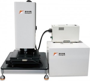
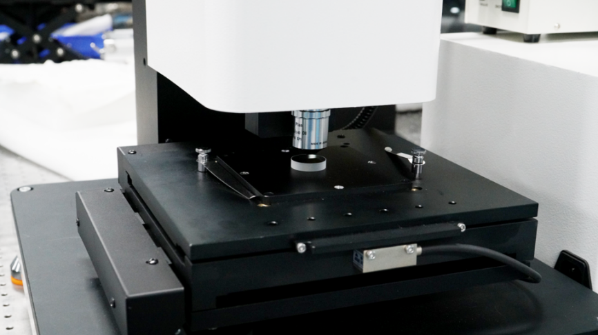
Wavelength OE’s new industrial white light interferometer features dual interferometry measurement modes. With non-contact detection, it covers full workflow from laboratory R&D to online production QC.
Dual Core Interferometry Modes for All Surface Topography
Unlike single-mode measuring devices, this system integrates VSI (Vertical Scanning Interferometry) and PSI (Phase-Shifting Interferometry) algorithms, satisfying two core measurement demands with one machine.
| Comparison Item | VSI / CSI | PSI |
|---|---|---|
| Main Applicable Surfaces | Rough surfaces, steps, discontinuous & complex topographies | Ultra-smooth, continuous and mirror surfaces |
| Vertical Height Measurement Range | Wide range; capable of measuring deep grooves and high steps | Narrow range; not suitable for isolated large steps |
| Vertical Resolution | Nanometer level; sub-nanometer achievable with optimized algorithms | Highest resolution; repeatability down to sub-nanometer even sub-angstrom level |
| Tolerance to Surface Roughness | High | Low |
| Phase Ambiguity | Nearly none; absolute height value output available | Subject to 2π phase wrapping error |
| Measuring Speed | Requires axial scanning, relatively slow | Generally faster |
| Vibration Resistance | Susceptible to vibration during scanning | Multi-frame phase shifting, more sensitive to vibration |
| Typical Applications | Roughness, step height, microstructures, machined surfaces | Ultra-smooth surface roughness, surface figure & flatness testing |
PSI (Phase-Shifting Interferometry): Specialized in nano-scale tiny height features and ultra-thin films, delivering ultimate microscopic resolution.
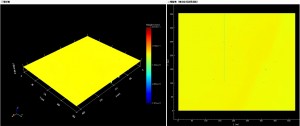
Plane Mirror
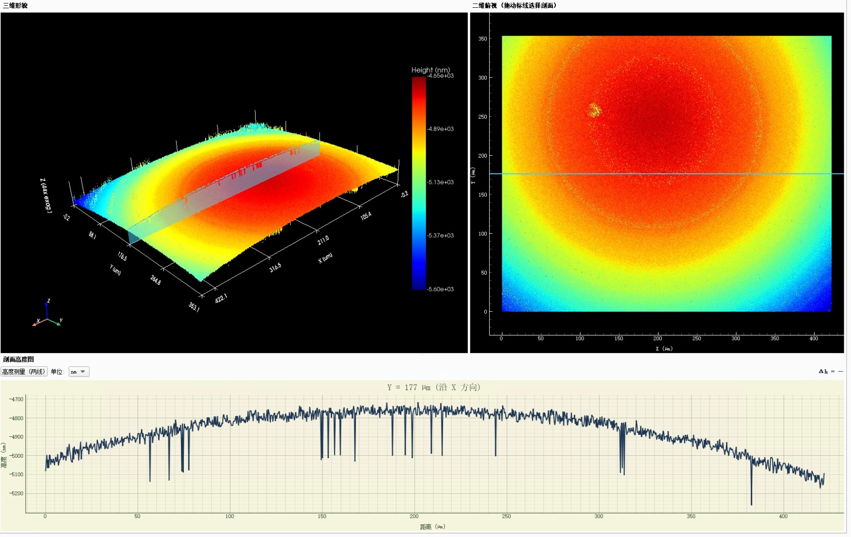
Curved Mirror(Convex Mirror)
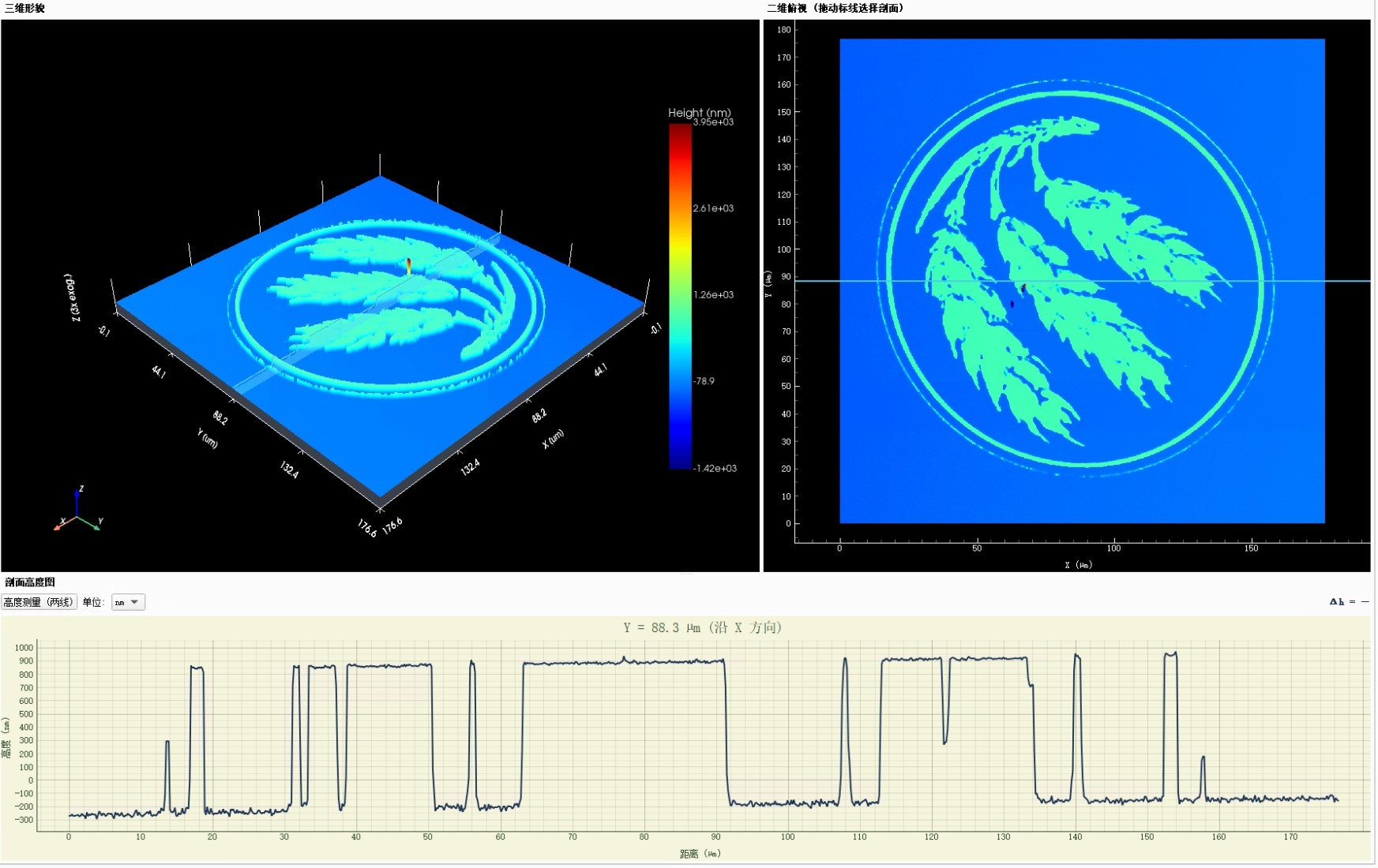
Photolithographic Pattern Sample
VSI Vertical Scanning Interferometry: Optimized for workpieces with large height variations and tall steps; full measuring range available without segmented scanning.
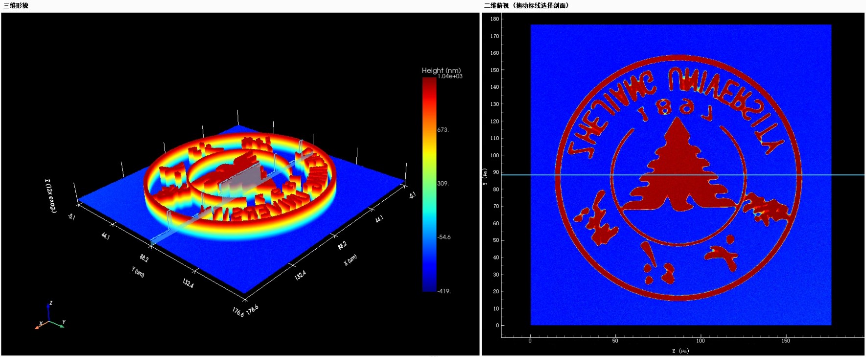
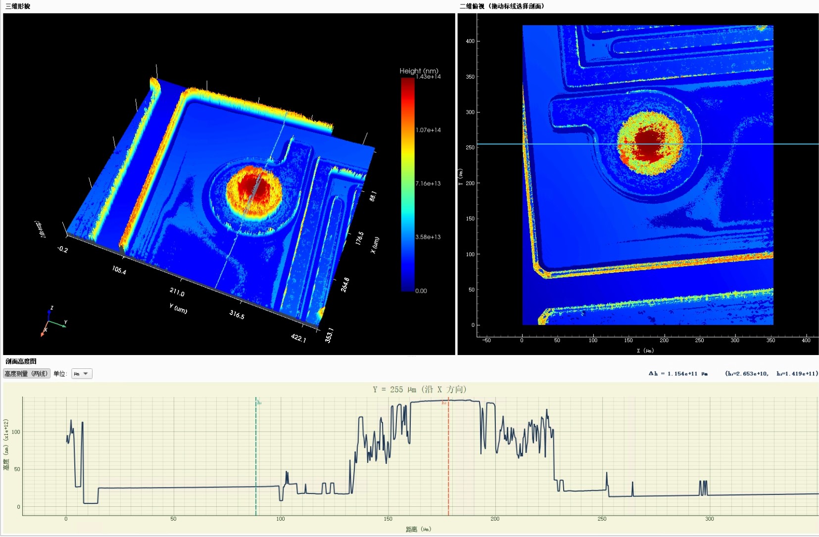
Circular micro bump array on advanced packaged wafers
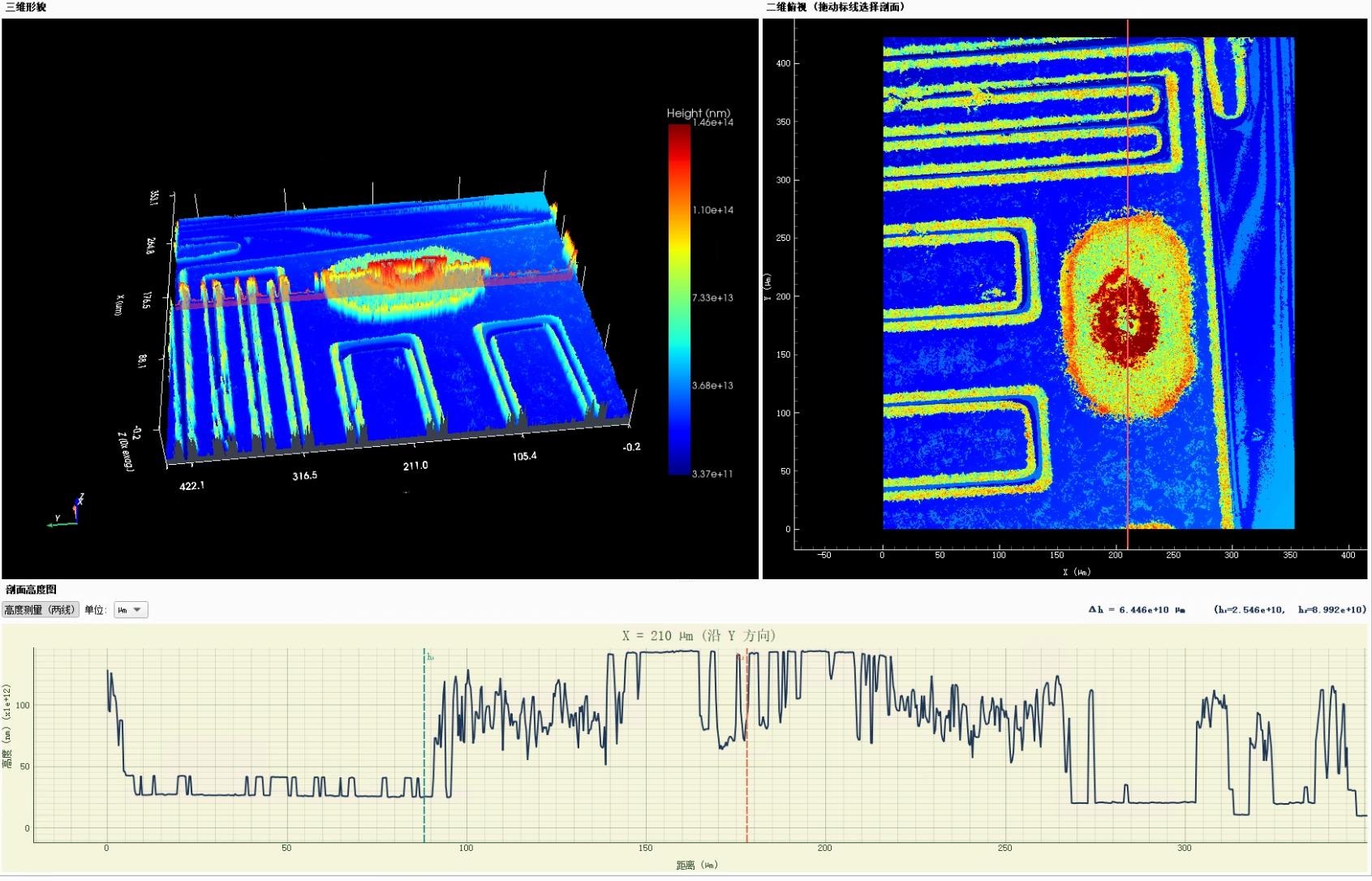
Elliptical micro bump array on advanced packaged wafers
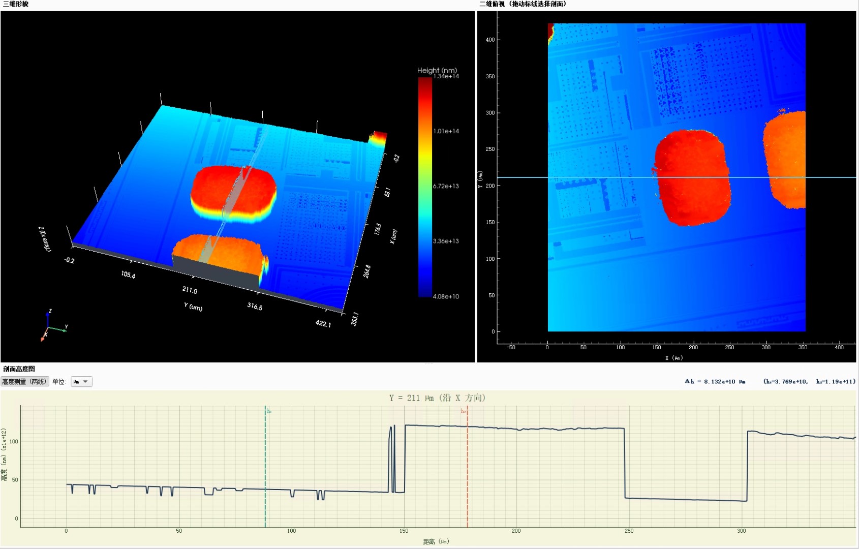
microlens array
Matched with a 450–700 nm short-coherence white light source, it can effectively suppress stray light from multiple reflections and delivers strong anti-interference performance. Equipped with multi-layer coatings, this optical component with low reflectivity can output stable and distinct interference signals, yielding authentic and reliable measurement results.
2. Industry-Leading Nano-Grade Specifications, Traceable & Stable Long-Term Data
-The system adopts an LED white light source with central wavelength at 550 nm, equipped with top-tier core performance parameters matching global premium standards.
-Vertical resolution: <1 nm, repeat measurement error: <10 nm, true nanometer precision
-Maximum vertical measuring range: 500 μm, no repeated repositioning required for high-low microstructures.
-Scanning speed: 100 μm/s, single full scan completed within 10 seconds, balancing precision and inspection throughput.
-Compliant with NIST traceable standards, built-in auto-calibration algorithm ensures consistent traceable batch data, meeting strict QC standards for semiconductor and optical industries.
| Item | Parameter |
| Measuring Capacity | 3D surface topography, surface roughness, step height & film thickness of reflective materials and optical components |
| Data Acquisition Mode | Vertical Scanning Interferometry (VSI) + Phase-Shifting Interferometry (PSI) |
| Calibration System | NIST traceable standard + automatic calibration algorithm |
| Vertical Measuring Range | 500 μm |
| Field of View | 20× objective: 0.87 × 0.65 mm |
| Camera Performance | Max Resolution: 2048×2448; Frame Rate: 74 Fps; Bit Depth: 12 bit |
| Scanning Speed | 100 μm/s (Precision Mode) |
| Objective Lens Options | Configurable 20x / 50x magnification objectives |
| Installation Design | Built-in active vibration isolation platform, horizontal & vertical mounting available |
| Overall Dimension (L×W×H) | 120 × 80 × 65 cm |
| Net Weight | ≤58 kg |
3. Industrial Integrated Cabinet Design, Compatible with Lab & Production Line
Optimized for both mass manufacturing workshops and scientific research labs with flexible installation compatibility.
Built-in active vibration isolation platform: Stable measurement under factory vibration, no extra vibration isolation table needed.
Dual mounting structure: Horizontal or vertical setup, easy integration with automated production lines and lab workstations.
Compact all-in-one body: Small footprint with dimension 120×80×65 cm, weight ≤58 kg, simple on-site deployment.
The complete system integrates light source, interferometer main unit and control module. Plug-and-play after unpacking, no complicated optical path adjustment required.
Wide Application Coverage for High-Precision Manufacturing
Semiconductor Industry: 3D topography & step height inspection of silicon wafers and micro-nano chips.
Precision Optics: Roughness and film thickness testing for optical lenses, objectives and coated optical elements.
New Functional Coatings: Surface profile and thickness analysis of reflective coatings & functional thin films.
Scientific Research Labs: Micro-nano structure characterization & precision component morphology testing.
With years of professional experience in optical R&D,Wavelength OE independently develops all core optical paths and measurement algorithms for white light interferometers. Full technical control from light sources, objective lenses to calibration systems. Every unit undergoes multi-round precision calibration before delivery. We provide full after-sales technical support and customize exclusive measuring solutions based on customer workpiece size and automatic production line requirements.
Post time: Jul-15-2026