
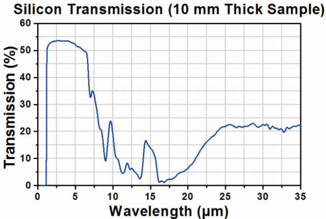
Single crystal silicon (Si) is a chemically inert material with high hardness and insolubility in water. It offers excellent transmission in the 1.2–7 μm waveband and also in the far-infrared range from 300 to 300 μm, a feature not commonly found in other infrared materials. Single crystal silicon (Si) is typically used for 3–5 μm mid-wave infrared (MWIR) optical windows and optical filter substrates. Due to its good thermal conductivity and low density, it is also a commonly used material for laser mirrors. Single crystal silicon has a density of 2.316 g/cm³ and a Knoop hardness of 1150, making it harder and less brittle than germanium.
|
Parameter |
Value |
|
Lens Aperture Range |
4mm – 400mm |
|
Edge Thickness Range |
≥ 0.7mm |
|
Center Thickness Range |
≥ 1mm |
|
Processing Angle Range |
0° – 65° |
|
Sagitta (Sag) Range |
≤ 21mm |
|
PV (Surface Figure) |
0.1 μm |
|
Ra (Surface Roughness) |
2 nm – 6 nm |
|
ΔN (Surface Figure Error) |
0.3 – 1 |
Infrared silicon glass wafers are key components for infrared optical systems and are mainly used in thermal imaging, laser sensors, infrared thermometry, and other applications.
Below is an overview of related products and technical features.
I. Product Types
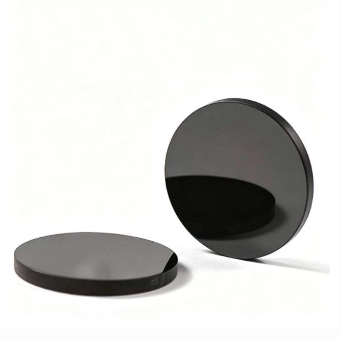
Standard Silicon Lenses
Single crystal silicon windows are suitable for infrared thermometers and sensors. Zone-refined silicon filters (coated) are used for pyroelectric sensors.
| Diameter (mm) | Thickness (mm) | Coating Requirement |
| 10 | 1 | 3–5 μm AR, T > 97% |
| 12.5 | 1 | 3–5 μm AR, T > 97% |
| 20 | 2 | 3–5 μm AR, T > 97% |
| 25 | 3 | 3–5 μm AR, T > 97% |
| 30 | 3 | 3–5 μm AR, T > 97% |
| 38.1 | 3 | 3–5 μm AR, T > 97% |
| 40 | 4 | 3–5 μm AR, T > 97% |
| 50 | 3 | 3–5 μm AR, T > 97% |
| 50.8 | 3 | 3–5 μm AR, T > 97% |
| 63.5 | 5 | 3–5 μm AR, T > 97% |
| 75 | 3 | 3–5 μm AR, T > 97% |
| 75 | 5 | 3–5 μm AR, T > 97% |
| 76.2 | 6 | 3–5 μm AR, T > 97% |
| 80 | 8 | 3–5 μm AR, T > 97% |
| 90 | 10 | 3–5 μm AR, T > 97% |
| 100 | 10 | 3–5 μm AR, T > 97% |
| 150 | 15 | 3–5 μm AR, T > 97% |
| 180 | 18 | 3–5 μm AR, T > 97% |
| 200 | 20 | 3–5 μm AR, T > 97% |
| 300 | 35 | 3–5 μm AR, T > 97% |
High-Precision Custom Lenses
Large-size high-precision silicon lenses are suitable for optical sensors. They are used in infrared imaging or surveillance, infrared thermometry, remote sensing, or infrared beam splitters and other optical systems. Their transmission spectral range is 1.2–7 μm, and they are commonly used in infrared optical systems.
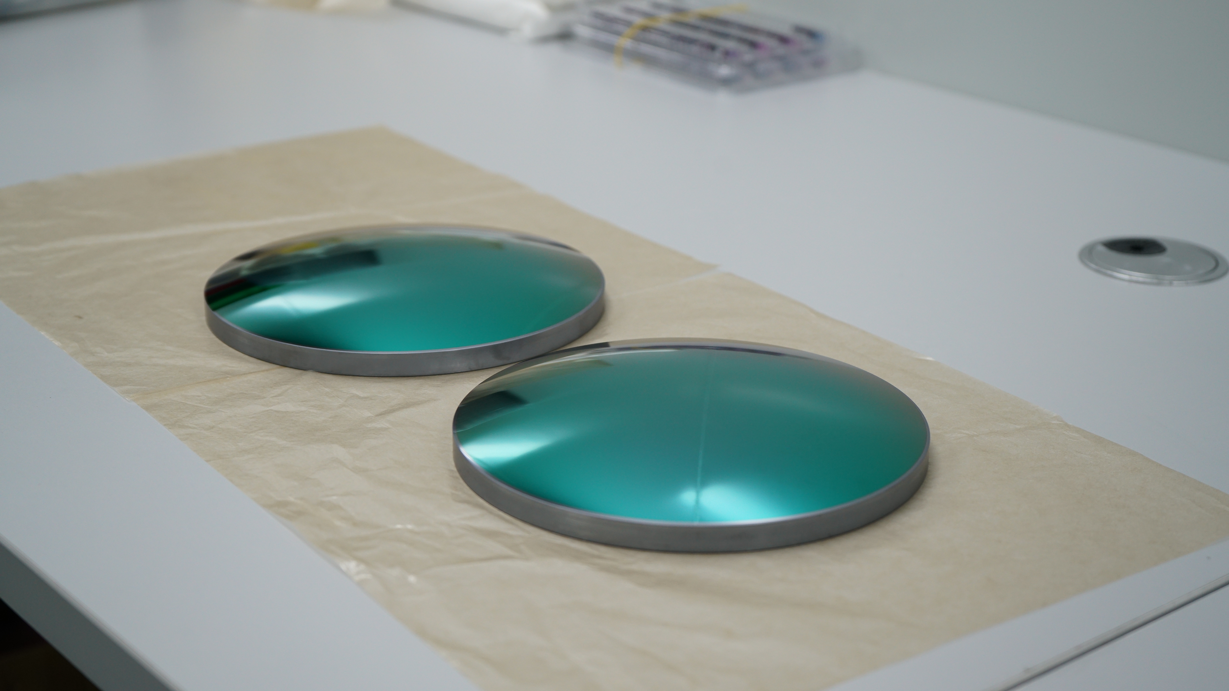
A 137 mm diameter silicon infrared component is a large-aperture infrared optical part made from single crystal silicon, widely used in MWIR imaging, LiDAR, semiconductor inspection, and other fields.
It uses high-purity single crystal silicon and offers high transmittance in the 1.2–7 μm waveband, especially in the 3–5 μm MWIR region. Its refractive index is approximately 3.4, and it features high thermal conductivity and a low coefficient of thermal expansion, making it suitable for high-power and wide-temperature applications.
This size falls within the large-size silicon processing range and provides good optical uniformity and thermal stability. It supports ultra-precision machining, with surface figure accuracy up to λ/10 (λ = 632.8 nm) and surface roughness Ra ≤ 2 nm, meeting the wavefront quality requirements of high-end optical systems.
The 137 mm diameter belongs to the customized large-size category and is suitable for large-field-of-view infrared imaging systems, space remote sensing lenses, and semiconductor wafer internal defect inspection equipment. It can be integrated into infrared lens barrels or microscopic imaging systems for through-silicon observation. Such components are often used as infrared windows, lenses, or prisms. Combined with single-point diamond turning and magnetorheological polishing, they ensure complex surface shapes and high surface figure accuracy and are key components of high-performance infrared systems.
Special Function Types
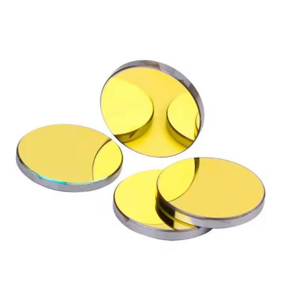
Gold-coated mirrors (e.g., single crystal high-resistivity silicon), available with hole drilling.
| Specifications | Value |
| Diameter Tolerance | +0/-0.13 mm |
| Thickness Tolerance | ±0.25 mm |
| Parallelism | ≤ 3 arc min. |
| Clear Aperture | > 90% |
| Surface Flatness | λ/4 per 1″ Dia @632.8 nm |
| Surface Quality | 40-20 S-D |
| Angle of Incidence | 45° |
| Part No. | Dia (mm) | Thk (mm) | Material | Wavelength (Remarks) |
| RSI-12-1.5 | 12 | 1.5 | Silicon | HR@10.6um |
| RSI-15-4 | 15 | 4 | Silicon | HR@10.6um |
| RSI-19-3E | 19 | 3 | Silicon | HR@10.6um |
| RSI-0.75-3 | 19.1 | 3 | Silicon | HR@10.6um |
| RSI-1-3 | 25.4 | 3 | Silicon | HR@10.6um |
| RSI-1-3DBR | 25.4 | 3 | Silicon | HR@10.6um/650nm |
| RSI-1.1-3 | 27.9 | 3 | Silicon | HR@10.6um |
| RSI-1.5-4 | 38.1 | 4 | Silicon | HR@10.6um |
| RSI-1.5-9.6 | 38.1 | 9.7 | Silicon | HR@10.6um |
| RSI-2-5 | 50.8 | 5.1 | Silicon | HR@10.6um |
| RSI-2-9.5 | 50.8 | 9.5 | Silicon | HR@10.6um |
| RMO-0.75-3 | 19 | 3 | Molybdenum | Polished surface |
| RMO-1-3 | 25.4 | 3 | Molybdenum | Polished surface |
Infrared-transmitting, visible-light-absorbing filters, which effectively block visible light and enhance infrared transmission performance.

II. Technical Characteristics
Coating technology: uncoated silicon lenses have a transmittance of about 45%, while AR-coated versions can reach 80%, significantly improving scratch resistance and corrosion resistance.
Material advantages: silicon (Si) substrates offer good thermal conductivity and low density, making them suitable for laser mirrors and thermal imager windows.
IV. Selection Recommendations
Select the substrate (such as silicon, germanium, or chalcogenide glass) according to the waveband requirements. Coated products are preferred to improve transmittance and durability.
The refractive index characteristics of infrared silicon glass wafers mainly depend on the material composition and operating waveband. Key information is summarized below.
1. Refractive Index Characteristics of Silicon Materials
Typical value: the refractive index of silicon in the infrared band is approximately 3.4 (at a wavelength of 10 μm). Its high refractive index is mainly determined by the material’s electronic polarization and lattice vibration characteristics.
Temperature effect: the thermo-optic coefficient (dn/dT) of silicon is not a constant but varies with wavelength and temperature range. Literature data show that the thermo-optic coefficient of silicon at 1.5 μm and 20°C is approximately 1.87 × 10⁻⁴ K⁻¹; in the terahertz band, it is approximately 1.86 × 10⁻⁴ K⁻¹. In actual design, the temperature drift effect must be checked according to the specific operating waveband.
2. Refractive Index Test Standards for Infrared Glass
Test methods: GB/T 42657-2023 specifies the determination of the temperature coefficient of refractive index of infrared glass in the 2–13 μm band using the normal incidence method; GB/T 34184-2017 specifies the determination of the room-temperature refractive index of infrared glass using the deviation angle method. The two standards measure different physical quantities and should be selected according to actual requirements.
Uniformity requirements: refractive index inhomogeneity can cause optical wavefront distortion and must be controlled through precision inspection.
3. Application Scenario Differences
Waveband adaptation: the practical transmission window of silicon is usually 1.2–7 μm (limited by bandgap absorption and lattice absorption). Coating effect: after applying a high-efficiency anti-reflection coating, the average transmittance of silicon in the 3–5 μm band can reach approximately 90%–96% (limited by coating design and absorption/scattering; the theoretical 100% cannot be achieved).
4. Material Properties
Single crystal silicon: chemically inert and high in hardness, with excellent transmission in the 1–7 μm band. In addition, high-resistivity single crystal silicon has unique transmission advantages in the far-infrared/terahertz bands (from tens of microns to the millimeter scale).
Coating optimization: anti-reflection coatings (such as diamond films and Y₂O₃ films) can significantly improve transmittance in specific infrared bands (for example, diamond films show a very obvious anti-reflection effect in the 8–14 μm band). The specific transmittance peak depends on film thickness, deposition process, and substrate treatment; actual test data should be used as the reference.
5. Application Scenarios
Sensor field: laser mirrors, infrared thermometers, and thermal imager windows.
Special requirements: the detector response band must be matched (for example, cooled and uncooled detectors have different requirements for bands above 12 μm).
Post time: Oct-28-2026