
Wafer annealing is a critical process in semiconductor manufacturing, encompassing dopant activation, lattice restoration, and ultra-shallow junction (USJ) formation. Conventional furnace annealing and rapid thermal processing (RTP) suffer from high thermal budgets, poorly controlled dopant diffusion, and insufficient uniformity, rendering them inadequate for advanced technology nodes at 7 nm, 5 nm, and beyond—particularly for Gate-All-Around (GAA) architectures and 3D NAND flash memory. Laser-based wafer annealing, with its transient high-energy irradiation, micron-scale spatial precision, and minimal thermal diffusion, has emerged as the next-generation core process for meeting these demanding manufacturing requirements.
Core Principle of Laser Heating
The Wave Optics laser heating head features a proprietary optical design that delivers high-energy, thermally uniform laser beams for precision irradiation of wafer surfaces. The green laser offers excellent absorption matching with silicon-based materials (including SiC), enabling high-efficiency thermal treatment without damaging the wafer. This facilitates recrystallization of the ion-implanted damaged layer and efficient dopant activation. Subsequently, the substrate’s high thermal conductivity enables ultra-fast cooling, which freezes the lattice structure and suppresses dopant diffusion. This process successfully produces ultra-shallow junctions with both high activation efficiency and a steep (abrupt) junction profile.
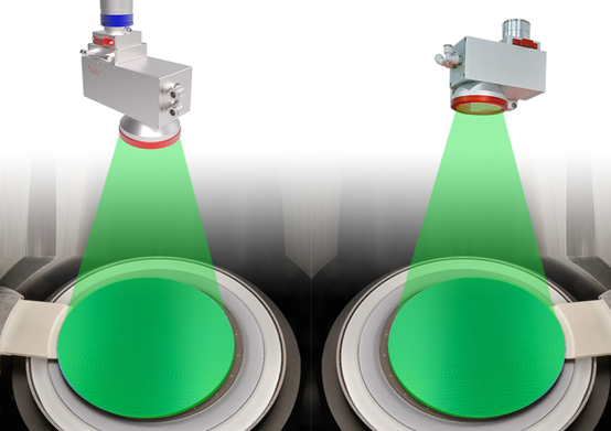
Laser Heating Annealing Is Critical for Improving Wafer Processing Yield
- Beam Uniformity: The energy uniformity of the flat-top beam spot exceeds 95% (typical), eliminating local over-melting or under-annealing.
- Energy Stability: Continuous output energy fluctuation is below 2%, ensuring excellent wafer-to-wafer and batch-to-batch consistency.
- Surface Figure Precision: Optical components feature nanometer-scale PV/RMS values with well-controlled wavefront distortion, preventing hot-spot damage.
- Depth of Focus and Beam Shaping: Customizable depth of focus combined with beam integrator homogenization supports full-field scanning of large-diameter wafers.
- Wavelength Matching: Optimized for high-absorption wavebands of silicon and third-generation semiconductors (e.g., SiC, GaN) to maximize energy utilization efficiency.
Three Key Advantages over Conventional Annealing
1.Excellent suppression of dopant diffusion -Thermal exposure is limited to the nanosecond-to-millisecond range with near-zero dopant diffusion, a capability unattainable by furnace annealing or RTP.
2.Low thermal budget and minimal device damage-Only the wafer surface experiences transient high temperatures, resulting in no thermal deformation of the substrate or device structures and no interfacial degradation.
3.Precision selective-area annealing -Tunable micron-scale beam spots support localized annealing for 3D integration and heterogeneous integrated devices.
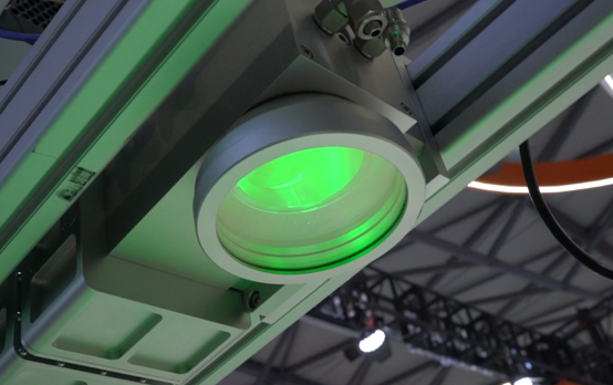
Application Scenarios
Applications include source/drain activation, channel repair, and ohmic contact annealing for advanced logic (GAA/CFET), DRAM/3D NAND, SiC/GaN power devices, SOI, and micro/nano devices. Laser annealing delivers simultaneous improvements in yield and device performance.
Laser annealing shifts wafer processing from global (blanket) annealing to precision local annealing. Its powerful optical technology supports the continued scaling and performance breakthroughs of advanced semiconductor nodes.
Product Specification Sheet
| Parameter | Specification |
| Power | 60-20000W |
| Wavelength | Customizable: 355/450/532/915/980/1080nm and other wavebands |
| Numerical Aperture (NA) | Customizable |
| Effective Homogenization Area | Customizable |
| Focal Length | ≥500mm (affected by the homogenization area) |
| Cooling | Water Cooling |
| Weight | 10kg |
| Dimensions | Customizable |
| Others | Optional: Infrared temperature field detection module, protective mirror contamination detection module |
Post time: Jul-23-2026