
Objective Introduction
Wavelength Opto-Electronic’s large-field industrial microscope objectives are manufactured with high-quality optical glass and anti-reflection coatings, significantly improving light throughput. The plan apochromatic design delivers crisp imaging details and high contrast. Built on an infinity-corrected optical system with a parfocal distance of 95 mm, these objectives are designed for brightfield coaxial illumination. They enable large-field observation, supporting an image circle diameter up to 40 mm, facilitating integration with various accessories and adaptation to complex working conditions. They are widely used in precision metrology and inspection in the semiconductor industry, as well as high-precision visual analysis and quality monitoring across diverse industrial applications.
Product Portfolio
Brightfield Microscope Objectives
Designed specifically for coaxial brightfield imaging, these objectives feature a plan apochromatic optical configuration, delivering high imaging contrast and large-field observation capability, with a maximum image circle diameter of 40 mm.
NUV Plan Apo 20X
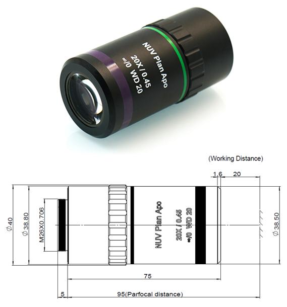
| Specification | Parameter | Specification | Parameter |
| Magnification (X) | 20X | Numerical Aperture (NA) | 0.45 |
| Working Distance (WD) | 20mm | Focal Length | 10mm |
| Resolution | 0.75μm | Depth of Focus (±D.F) | 1.65μm |
| Parfocal Distance | 95mm | Entrance Pupil Diameter | 9mm |
| Field of View (MAX) | 2mm | Working Wavelength | 355-700nm |
| Mounting Thread | M26×0.706 | Weight | 373g |
M Plan Apo 2X
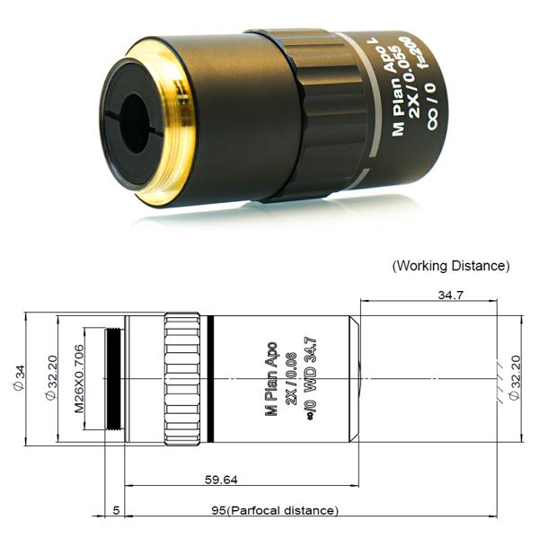
| Specification | Parameter | Specification | Parameter |
| Magnification (X) | 2X | Numerical Aperture (NA) | 0.06 |
| Working Distance (WD) | 34.7mm | Focal Length | 100mm |
| Resolution | 5.6μm | Depth of Focus (±D.F) | 93.2μm |
| Parfocal Distance | 95mm | Entrance Pupil Diameter | 12mm |
| Field of View (MAX) | 18mm | Working Wavelength | 380-700nm |
| Mounting Thread | M26×0.706 | Weight | 208g |
M Plan Apo 5X
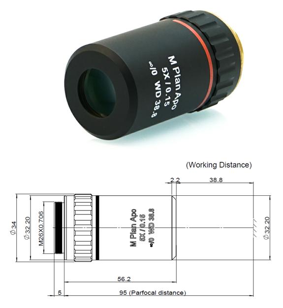
| Specification | Parameter | Specification | Parameter |
| Magnification (X) | 5X | Numerical Aperture (NA) | 0.15 |
| Working Distance (WD) | 38.8mm | Focal Length | 40mm |
| Resolution | 2.2μm | Depth of Focus (±D.F) | 14.9μm |
| Parfocal Distance | 95mm | Entrance Pupil Diameter | 12mm |
| Field of View (MAX) | 8mm | Working Wavelength | 380-700nm |
| Mounting Thread | M26×0.706 | Weight | 233g |
M Plan Apo 10X
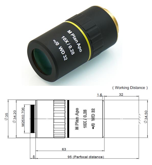
| Specification | Parameter | Specification | Parameter |
| Magnification (X) | 10X | Numerical Aperture (NA) | 0.28 |
| Working Distance (WD) | 32mm | Focal Length | 20mm |
| Resolution | 1.2μm | Depth of Focus (±D.F) | 4.3μm |
| Parfocal Distance | 95mm | Entrance Pupil Diameter | 11.7mm |
| Field of View (MAX) | 4mm | Working Wavelength | 380-700nm |
| Mounting Thread | M26×0.706 | Weight | 244g |
M Plan Apo 20X
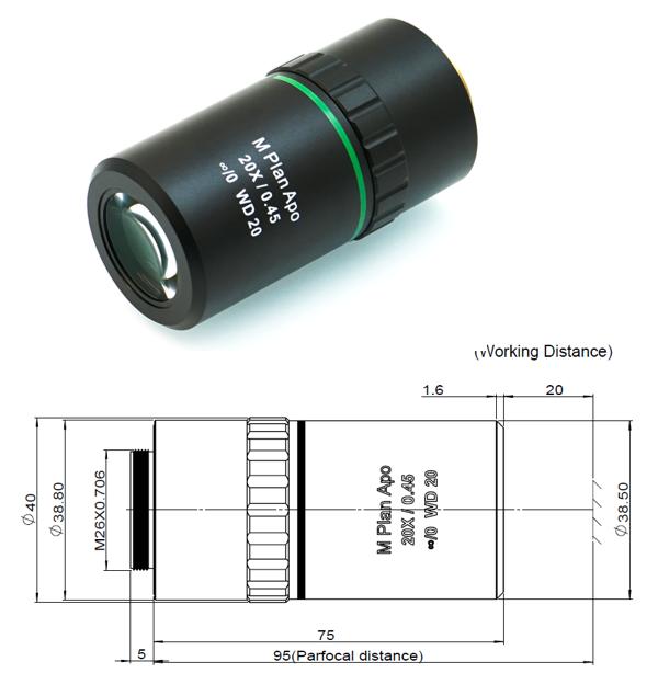
| Specification | Parameter | Specification | Parameter |
| Magnification (X) | 20X | Numerical Aperture (NA) | 0.45 |
| Working Distance (WD) | 20mm | Focal Length | 20mm |
| Resolution | 0.75μm | Depth of Focus (±D.F) | 1.65μm |
| Parfocal Distance | 95mm | Entrance Pupil Diameter | 9mm |
| Field of View (MAX) | 2mm | Working Wavelength | 380-700nm |
| Mounting Thread | M26×0.706 | Weight | 373g |
M Plan Apo 50X
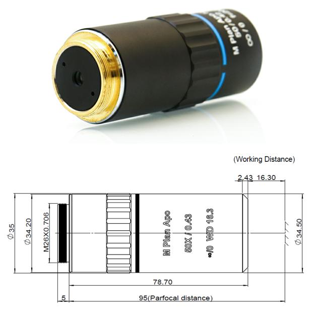
| Specification | Parameter | Specification | Parameter |
| Magnification (X) | 50X | Numerical Aperture (NA) | 0.43 |
| Working Distance (WD) | 16.3mm | Focal Length | 4mm |
| Resolution | 0.8μm | Depth of Focus (±D.F) | 1.8μm |
| Parfocal Distance | 95mm | Entrance Pupil Diameter | 3.44mm |
| Field of View (MAX) | 0.8mm | Working Wavelength | 380-700nm |
| Mounting Thread | M26×0.706 | Weight | 277g |
Darkfield Microscope Objectives
Designed for observing surface scattering and topography, these objectives feature a plan apochromatic optical configuration, delivering high imaging contrast and large-field observation capability, with a maximum image circle diameter of 40 mm.
M Plan Apo BD
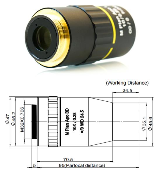
| Specification | Parameter | Specification | Parameter |
| Magnification (X) | 10X | Numerical Aperture (NA) | 0.28 |
| Working Distance (WD) | 24.5mm | Focal Length | 20mm |
| Resolution | 1.2μm | Depth of Focus (±D.F) | 4.3μm |
| Parfocal Distance | 95mm | Entrance Pupil Diameter | 11.7mm |
| Field of View (MAX) | 4mm | Working Wavelength | 380-700nm |
| Mounting Thread | M26×0.706 | Weight | 264g |
White-Light Interference Microscope Objectives
Designed for non-contact measurement of surface topography and geometric features, these objectives feature a plan apochromatic optical configuration with large-field observation capability, supporting an image circle diameter up to 40 mm.
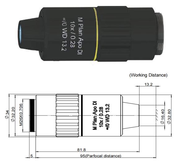
| Specification | Parameter | Specification | Parameter |
| Magnification (X) | 10X | Numerical Aperture (NA) | 0.28 |
| Working Distance (WD) | 13.2mm | Focal Length | 20mm |
| Resolution | 1.2μm | Depth of Focus (±D.F) | 4.3μm |
| Parfocal Distance | 95mm | Entrance Pupil Diameter | 11.7mm |
| Field of View (MAX) | 4mm | Working Wavelength | 380-700nm |
| Mounting Thread | M26×0.706 | Weight | 264g |
Application Fields
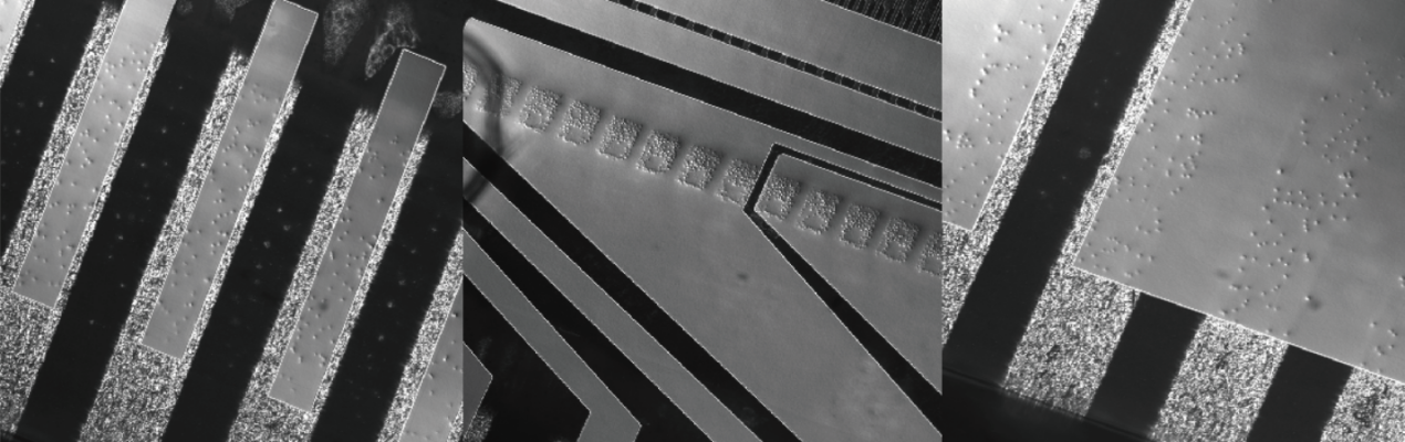
Semiconductor Manufacturing
In this field, Wavelength’s microscope objectives are primarily used for defect analysis, failure localization, and process monitoring.
Application Scenarios:
Defect Inspection and Classification: Identifying and classifying particles, scratches, crystal defects, etc., on wafer surfaces. High resolution and freedom from color artifacts ensure accurate defect feature recognition.
Failure Analysis: Locating short-circuit and open-circuit points in faulty chips. The planarity ensures that both edges and center remain equally sharp when searching for anomalous areas across a large field of view.
Critical Dimension Measurement: Performing sub-micron precision measurements of line widths, via diameters, etc., on integrated circuits. Superior image quality is the foundation for measurement accuracy.
Internal Inspection via Infrared Objectives: Dedicated plan apochromatic infrared objectives enable non-destructive internal inspection of packaged chips, as silicon material is transparent to infrared light.
Industrial Inspection
In the industrial sector, Wavelength’s microscope objectives are used for material analysis, quality control, and non-destructive testing.
Application Scenarios:
Materials Science: Analyzing grain structure, phase composition, and defects in metals, ceramics, and polymers. Apochromatic correction is essential for observing anisotropic materials under polarized light.
Precision Manufacturing: Inspecting wear, micro-cracks, and surface roughness on precision components (e.g., cutting tools, bearings). High resolution enables early detection of potential failure signs.
Electronics Industry: Checking solder joint quality and circuit integrity on PCBs. Planar objectives facilitate automated scanning and measurement across entire circuit boards.
Post time: Jul-30-2026