
Differential Interference Contrast (DIC) Microscope Lens


Differential Interference Contrast (DIC) Microscope Lens
Product Advantages
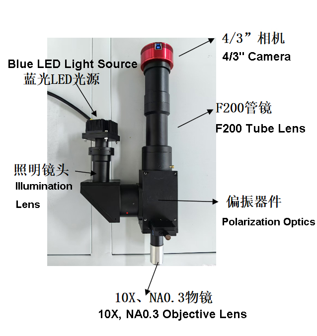
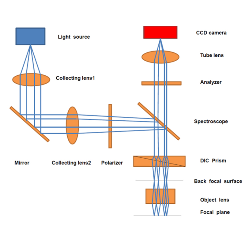
This system offers high-resolution, high-precision, non-contact, and non-destructive measurement. With resolution reaching the sub-nanometer level, it enables the observation of finer surface structures and topographical changes. Because the technique requires no physical contact with the sample, it eliminates the risk of sample damage and contamination, making it highly suitable for observing and researching biological and medical samples.
The microscope features a compact, stable, and highly rigid main body that meets the vibration isolation requirements for microscopic operations. Its modular design concept facilitates convenient system upgrades. The guide-pillar lifting mechanism allows for quick adjustment of the distance between the stage and the objective lens, making it suitable for inspecting workpieces of varying thicknesses.
Equipped with a mechanical moving stage, it ensures effective positioning of workpieces and is ideal for microscopic observation or rapid inspection of multiple samples. The ergonomic design provides more convenient and comfortable operation with a more spacious working area.

Parameter table:
| Magnification | 10X |
| Working Distance (WD) | 32 mm |
| Resolution | 1.2 um |
| Parfocal Distance | 95 mm |
| Max Field of View | 4 mm |
| Thread | M26X0.706 |
| Numerical Aperture (NA) | 0.28 |
| Focal Length | 20 mm |
| Depth of Field (D.F) | 4.3 um |
| Entrance Pupil Diameter | 11.7 mm |
| Working Wavelength | 380-700 nm |
| Weight | 244 g |
| Magnification | 7X |
| Working Distance (WD) | 37 mm |
| Resolution | 1.6 um |
| Parfocal Distance | 95 mm |
| Line Pairs | 625 lp/mm |
| Objective Threading | M26X0.706 |
| Numerical Aperture (NA) | 0.22 |
| Focal Length | 28.6 mm |
| Cover Glass Thickness | None |
| Transmittance | 87% |
| Working Wavelength | 400-700 nm |
Application of DIC microscope:
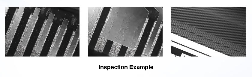
- 1.Biological Imaging: Enables non-invasive, dye-free observation of live cells. Combines with fluorescence for tracking cell dynamics and provides pseudo-3D views for structural analysis of tissues and microorganisms.
- 2.Semiconductor Inspection: Detects microscale defects and residues on wafers and PCBs. Offers non-contact surface uniformity measurement and real-time process monitoring to improve manufacturing yield.
- 3.Materials & Nanotechnology: Characterizes surface topography (roughness, phase separation) of metals and polymers. Monitors pattern fidelity in nanofabrication processes.
- 4.Precision Engineering: Inspects precision components for scratches and pits. Aids in dimensional analysis of MEMS and provides high-resolution PCB defect inspection (solder joints, vias, cracks).

PRODUCT CATEGORIES
Wavelength has been focused on providing high precision optical products for 20 years


