
Femtosecond laser pulses have extremely short durations and extremely high peak powers, capable of vaporizing hard ceramics, reshaping corneal tissue without burning it, and driving nonlinear optical effects. These characteristics impose stringent requirements on optical components: if mirrors, lenses, and windows are not manufactured to femtosecond standards, the pulse will degrade before reaching the workpiece.
1. Why Femtosecond Laser Optics Differs from Conventional Optics
Conventional optical components for continuous-wave or nanosecond-pulse systems have relatively relaxed design requirements: achieving coated reflection or transmission at the appropriate wavelength, maintaining a surface smooth enough to avoid scattering, and ensuring a damage threshold well above the operating power. Femtosecond systems, by contrast, operate under two dominant constraints: damage threshold and dispersion.
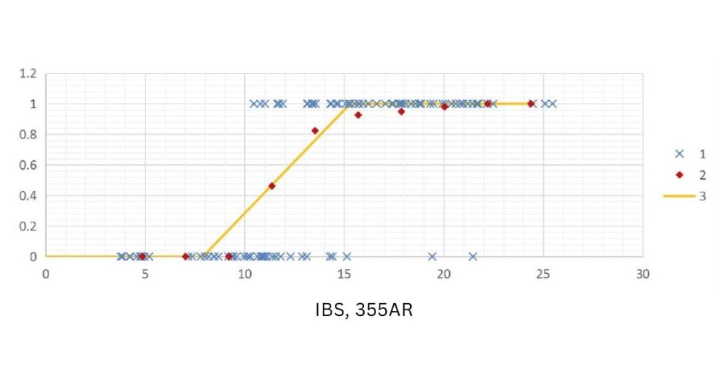
Damage threshold: Femtosecond pulses concentrate energy into an extremely short time window, so their peak intensity can be orders of magnitude higher than that of nanosecond pulses with the same average power. The laser-induced damage threshold (LIDT) required for femtosecond optics is typically only one-tenth to one-twentieth of that for nanosecond systems, even though the peak power density is two to three orders of magnitude higher. For this reason, femtosecond optics cannot simply be regarded as upgraded versions of standard laser mirrors; they require fundamentally different approaches to coating design, substrate purity, and surface finish.
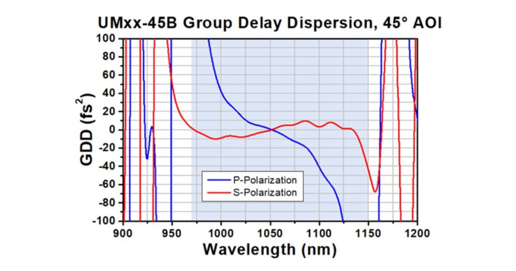
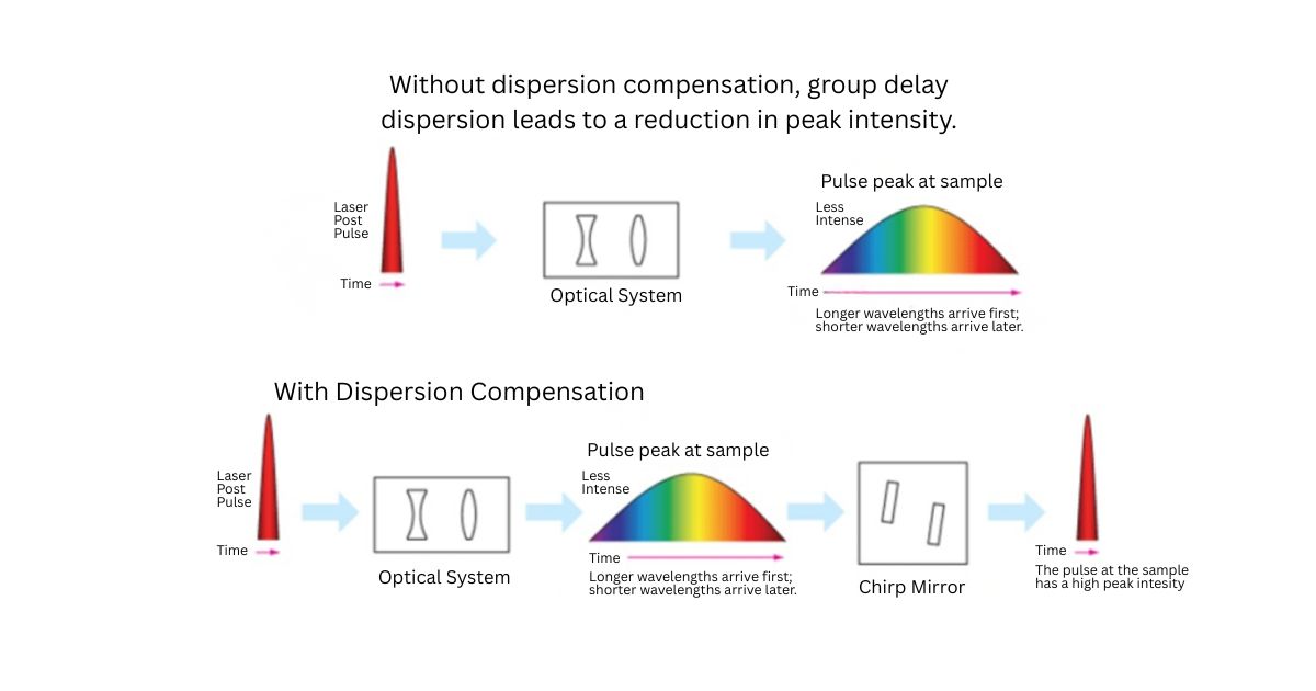
Dispersion: Different wavelengths propagate at slightly different speeds in any transparent material. For nanosecond pulses, the spectral bandwidth is extremely narrow and dispersion is negligible; femtosecond pulses are inherently broadband—the shorter the pulse, the broader the wavelength range—so dispersion has a significant impact. A 50-femtosecond pulse passing through a few millimeters of ordinary optical glass may have its duration stretched several-fold, reducing peak power and processing precision. Controlling group delay dispersion (GDD) is a core engineering challenge, requiring careful substrate selection, special coating structures, and dedicated dispersion-compensation components.
Surface precision: Femtosecond optics place extremely high demands on surface figure accuracy, wavefront error control, and coating uniformity. In systems with multiple optical elements in series, tiny defects accumulate into significant phase distortion by the time the beam reaches the target, degrading spot quality and processing precision. The surface figure accuracy of critical femtosecond components is typically controlled to within a fraction of a wavelength.
2. Key Optical Components for Femtosecond Laser Systems
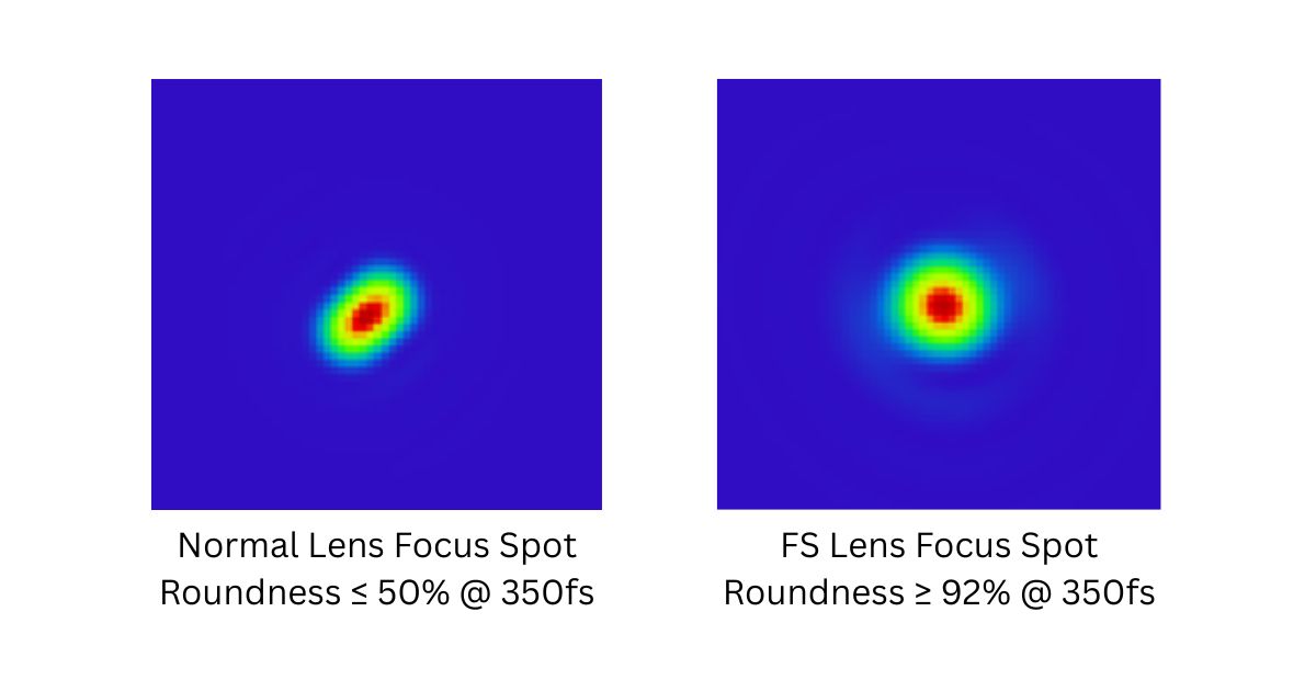
Beam delivery and focusing optics(lenses, windows, and steering mirrors)—require sufficiently precise control of surface figure and roughness to avoid introducing their own phase errors, along with damage threshold performance matched to the peak intensity. In scanning applications such as laser marking or micromachining, ultrafast Fθ lenses are far more important than commonly assumed: a standard Fθ lens optimized for a single wavelength severely distorts focusing quality when fed broadband femtosecond pulses, whereas a properly designed ultrafast Fθ lens maintains spot circularity and edge sharpness across the entire scan field.
Oscillator cavity mirrors must simultaneously provide extremely high reflectivity, near-zero group delay dispersion, and a damage threshold capable of withstanding continuous pulse circulation; intracavity wave plates require broad bandwidth and minimal added dispersion.
Amplifier stages impose their own set of optical requirements: gain crystals that manage thermal load without distorting the beam, pump coupling lenses with high damage thresholds and precise numerical aperture matching, and optical isolators that prevent back-reflections from destabilizing the seed oscillator.
Dispersion-compensation optics represent the true complexity of femtosecond engineering. Chirped mirrors use multilayer dielectric coatings designed so that different wavelengths penetrate to different depths before reflection, introducing precisely controlled negative dispersion to cancel the positive dispersion accumulated elsewhere in the system. Grating pairs and prism pairs provide similar tunable compensation and are particularly common in chirped-pulse amplification (CPA) systems, where pulses are intentionally stretched before amplification and recompressed afterward to avoid damaging the amplifier.
Nonlinear optical crystals such as BBO, LBO, KTP, and MgO-doped lithium niobate are used for wavelength-conversion processes including second- and third-harmonic generation. These processes require precise phase matching, strong nonlinear response, and the ability to withstand peak intensities far beyond the design limits of conventional laser crystals.
3. Main Application Areas
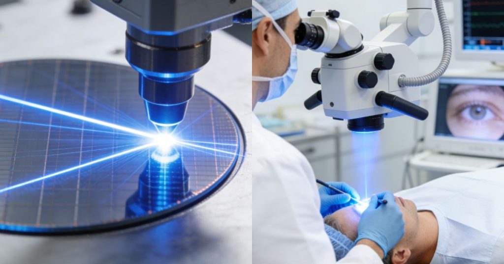
Precision manufacturing and electronics: OLED/LCD glass cutting, sapphire and ceramic cover-glass drilling, PCB via processing, and ultrathin copper foil etching all rest on the femtosecond “cold ablation” mechanism—material is removed faster than heat can conduct outward, so cracking, burrs, and discoloration do not occur.
Scientific research: Frontier techniques such as multiphoton microscopy, ultrafast spectroscopy, and frequency-comb metrology require complex optical paths that simultaneously preserve pulse width and beam quality, making dispersion-managed components indispensable rather than optional.
Medical and ophthalmic: Bladeless corneal cutting in LASIK is the most widely known case; in addition, fine processing of vascular stents, microfluidic chips, and interventional catheters also relies on femtosecond lasers, because surrounding tissue or fragile structures must never suffer thermal damage.
Semiconductor and battery fabrication: From wafer dicing and laser direct writing to chip packaging and through-silicon via etching, the value of femtosecond processing lies in a near-zero heat-affected zone; lithium battery tabs and electrodes likewise benefit in cutting and welding, where thermal damage to neighboring structures is impermissible.
4. Selection Considerations
Is the coating process suitable for ultrafast requirements? Not all coating technologies can simultaneously achieve the high reflectivity, ultralow absorption, and precise dispersion control required for femtosecond optics—this is where suppliers genuinely differ.
Was the damage threshold data measured under conditions similar to your application—comparable pulse duration, repetition rate, and spot size—rather than being a generic headline figure?
Does the supplier provide complete optical and dimensional metrology data for each component, so you can verify performance rather than simply trusting a specification sheet?
Does the GDD specification cover your actual operating bandwidth, rather than just a single wavelength?
Are the surface figure and roughness tolerances tight enough to avoid measurable wavefront distortion when combined with the rest of the beam path?
Does the supplier provide complete optical and dimensional metrology data for each component, so you can verify performance rather than simply trusting a specification sheet?
5.Where Wavelength Opto-Electronic Fits
Our company has established a vertically integrated production chain built specifically around ultrafast laser requirements—covering substrate fabrication, coating, and metrology, all under one roof.
Substrate processing is designed for dispersion-sensitive applications: fused silica and N-BK7 are primarily used for the visible and near-infrared bands common in Ti:sapphire and Yb-based femtosecond laser systems, owing to their low dispersion and high damage resistance, while materials such as calcium fluoride or magnesium fluoride are used for UV and IR applications. The manufacturing center employs advanced techniques such as magnetorheological finishing and ion beam processing to control surface figure accuracy to within a fraction of a wavelength—precision that directly reduces accumulated wavefront distortion along the femtosecond beam path.
Coating uses ion beam sputtering (IBS) technology—a denser, more tightly controlled deposition process—because standard evaporation coating processes cannot reliably achieve the high reflectivity, ultralow absorption, and precisely controlled group delay dispersion required for femtosecond optics. This includes low-GDD mirrors and chirped mirrors designed specifically for dispersion compensation in ultrashort-pulse systems.
Metrology capabilities include non-contact profilometry for aspheric and freeform surfaces, white-light interferometry for sub-nanometer roughness measurement, and full-spectral characterization of coating performance—meaning products are delivered with real measurement data backing their specifications, not just catalog claims.
6.Our Ultrafast Optics Products?
low-GDD cavity mirrors for frequency-doubled Yb and Nd systems; chirped mirrors for pulse stretching compensation; broadband beamsplitters compatible with Ti:sapphire and Yb laser platforms; F-theta lenses designed to preserve focused spot quality across femtosecond bandwidth in scanning applications; and high-LIDT lenses and protective windows designed specifically to meet femtosecond damage threshold requirements, rather than being converted from general-purpose optics.
1. 1 Ultrafast F-Theta Scan Lenses

| Ultrafast F-Theta Scan Lenses | |||||||
| Model No. | Wavelength (nm) | Scan Field | EFL (mm) | Focus Spot (μm) | Input Aperture (mm) | GDD (fs²) | Mounting |
| TSLA-343-45-150-D10 | 343 | 45×45 | 150 | 13 | 10 | 5304 | Thread Mount |
| TSLA-344-100-280-D10 | 343 | 100×100 | 280 | 18 | 10 | 7584 | Flange Mount |
| TSLA-343-185-420-D14 | 343 | 185×185 | 420 | 29 | 14 | 13956 | Flange Mount |
| TSLA-343-200-500-D14-V1 | 343 | 200×200 | 500 | 32 | 14 | 12540 | Flange Mount |
| TSLA-343-400-980-D20 | 343 | 400×400 | 980 | 42 | 20 | 27312 | Flange Mount |
1.2 Ultrafast Low Group Delay Dispersion Mirrors
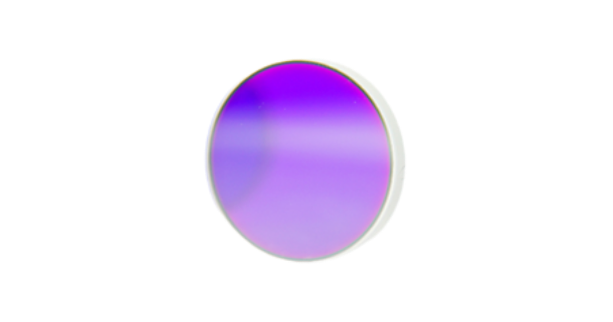
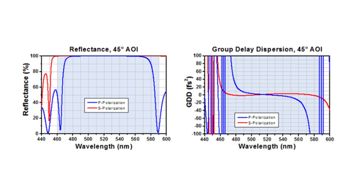
| Ultrafast Low Group Delay Dispersion Mirrors | ||
| Technical Requirements | 1/2″ (12.7 mm) | 1″ (25.4 mm) |
| Design Wavelength Range | 460 – 590 nm | |
| Diameter | 1/2″ (12.7 mm) | 1″ (25.4 mm) |
| Diameter Tolerance | +0.00 / -0.10 mm | |
| Thickness | 6.4 mm (0.25″) | 9.5 mm (0.37″) |
| Thickness Tolerance | ±0.20 mm | |
| Clear Aperture | >80% of diameter | |
| Reflectivity | Rs > 99% (460 – 590 nm) | |
| Rp > 99% (480 – 560 nm) | ||
| Angle of Incidence | 45° | |
| Group Delay Dispersion | |GDD_s| < 30 fs² (460 – 590 nm) | |
| |GDD_p| < 30 fs² (480 – 560 nm) | ||
| Substrate Material | Fused Silica | |
| Surface Figure | λ/10 @ 632.8 nm (within clear aperture) | |
| Surface Quality | 20-10 (scratch-dig) | |
1.3 Ultrafast High LIDT Lenses
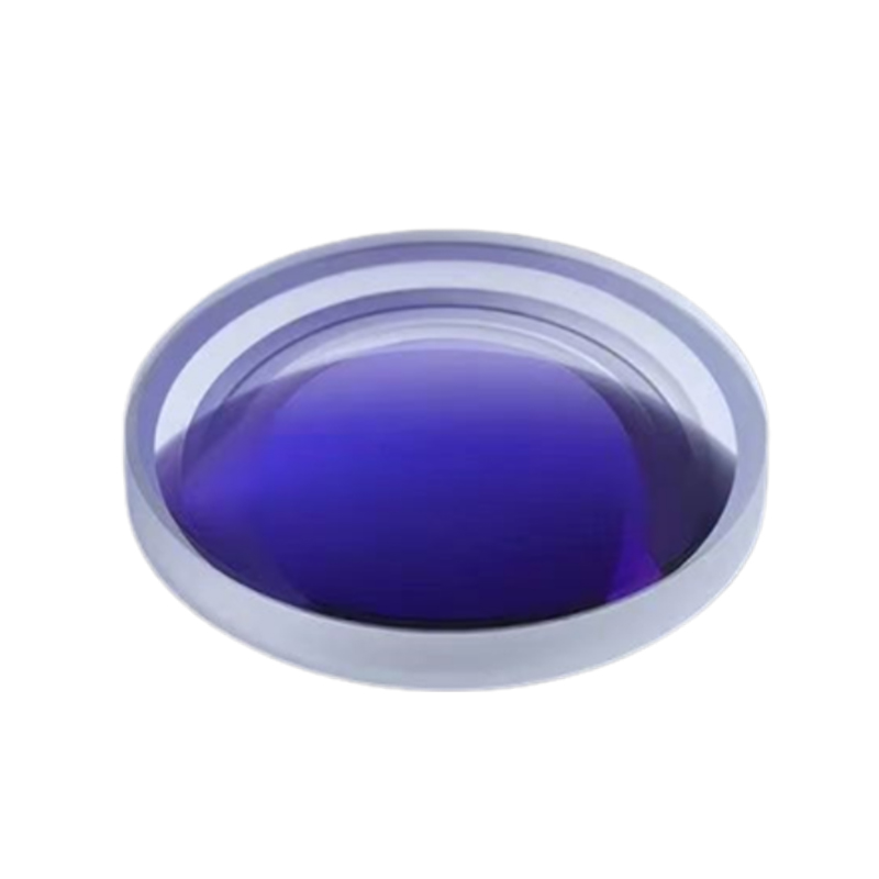
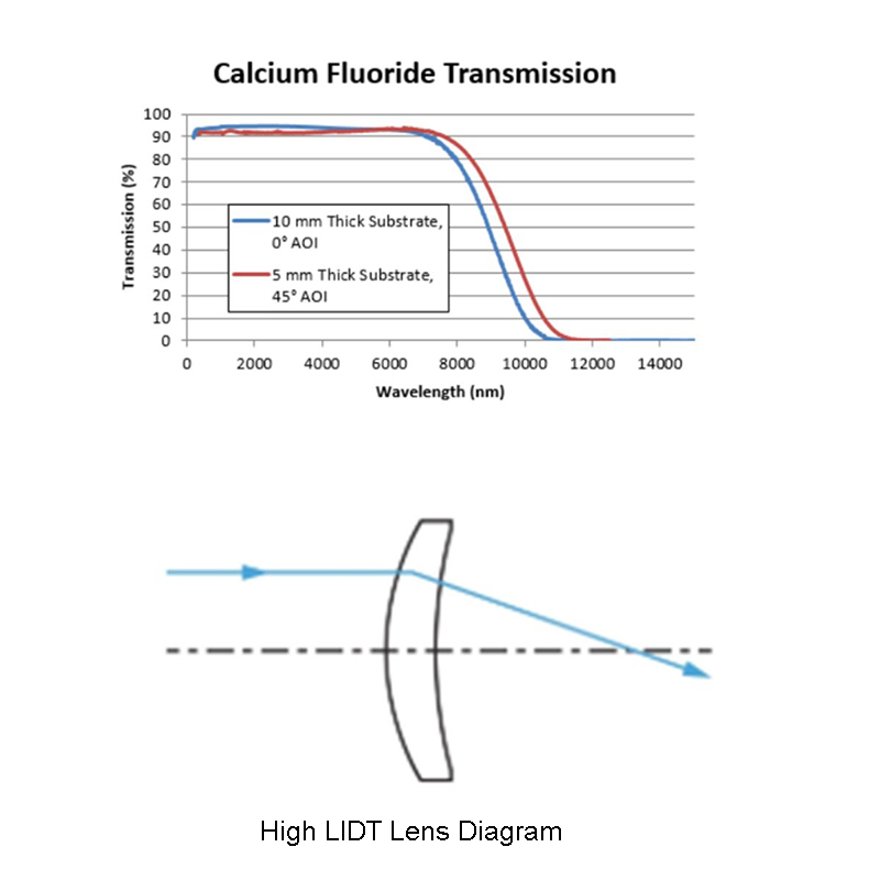
| Ultrafast High LIDT Lenses | |||
| Technical Requirements | Standard | Precision | High Precision |
| Shapes | Windows, plano-convex, plano-concave, double-convex, double-concave, spherical, aspherical, right-angle prisms, equilateral dispersive prisms, cylindrical lenses, wedge windows, beam splitters, UV laser objectives | ||
| Design wavelength | 0.18—8μm (high transmission) | ||
| Size | 10mm-80mm | ||
| Dimensional tolerance | ±0.1mm | ±0.025mm | ±0.01mm |
| Thickness tolerance | ±0.1mm | ±0.025mm | ±0.01mm |
| RMS roughness | < 15nm | < 7nm | < 3nm |
| Surface figure (@632.8 nm) | λ/2 | λ/4 | λ/10 |
| Surface quality | 40-20 | 46315 | 46300 |
1.4 Ultrafast Chirped Mirrors
| Ultrafast Chirped Mirrors | ||||
| Item | Parameter | |||
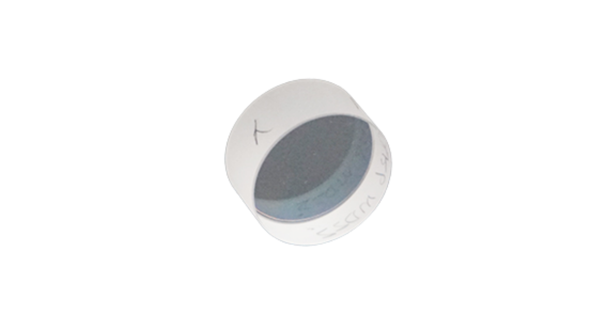
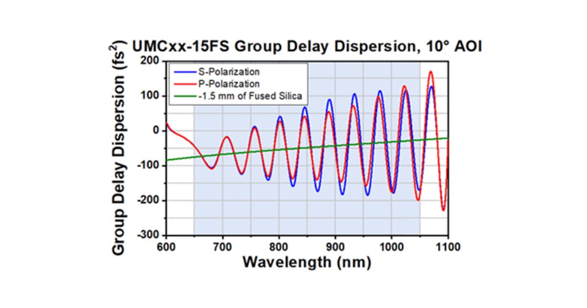
| Description | Chirped mirrors are employed for group delay dispersion (GDD) compensation, correcting pulse broadening occurring when ultrashort pulses traverse optical systems. | |||
| Reflectivity | Rabs >99.5% for each mirror across 650–1050 nm | |||
| Group Delay Dispersion (GDD) | -40 fs² @500–1000 nm | |||
| Clear Aperture (CA) | >80% over diameter | |||
| Angle of Incidence (AOI) | 10° | |||
| Applicable Pulse | Suitable for pulses with spectral bandwidth >50 nm FWHM | |||
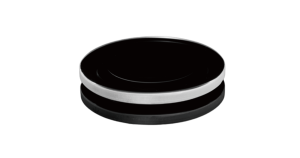
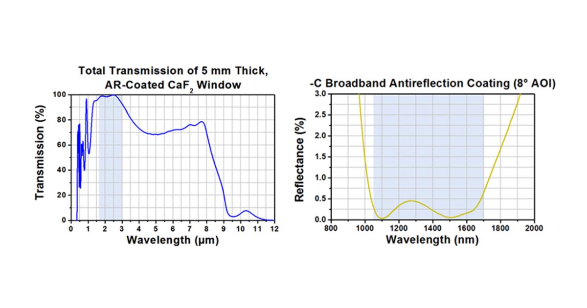
| Ultrafast High LIDT Laser Windows | |||
| Technical Requirements | Standard | Precision | High Precision |
| Substrate Material | N-BK7, Fused Silica, H-K9L, ZnSe | N-BK7, Fused Silica, H-K9L, ZnSe | N-BK7, Fused Silica, H-K9L, ZnSe |
| Design Wavelength | 0.2—10.6μm (high transmission) | 0.2—10.6μm (high transmission) | 0.2—10.6μm (high transmission) |
| Size Range | 10mm-300mm | 10mm-300mm | 10mm-300mm |
| Dimensional Tolerance | ±0.1mm | ±0.025mm | ±0.01mm |
| Thickness Tolerance | ±0.1mm | ±0.025mm | ±0.01mm |
| RMS Roughness | < 15nm | < 7nm | < 3nm |
| Surface Figure (@632.8 nm) | λ/2 | λ/4 | λ/10 |
| Surface Quality | 40-20 | 20-10 | 10-5 |
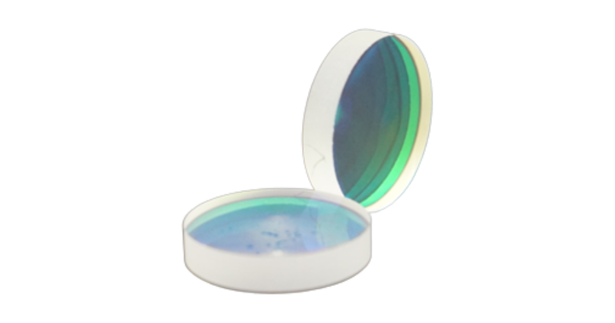
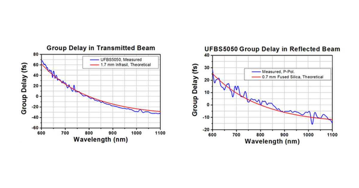
| Ultrafast Broadband Splitters | ||||
| Technical Requirements | 20/80 Ratio | 50/50 Ratio | 80/20 Ratio | 90/10 Ratio |
| Overall Performance | R_abs = 20 ± 2% | R_abs = 50 ± 5% | R_abs = 80 ± 5% | R_abs = 90 ± 2% |
| T_abs = 80 ± 2% | T_abs = 50 ± 5% | T_abs = 20 ± 5% | T_abs = 10 ± 2% | |
| Wavelength range | 600-1500 nm | |||
| AR Coating | Rabs < 0.5% @ 600 – 1500 nm | |||
| Dia Tol. | +0.00/-0.10 mm | |||
| Thickness Tol. | ±0.10 mm | |||
| Clear Aperture | >80% of Diameter | |||
| AOI | 45° | |||
| LIDT | 0.18 J/cm² (800 nm, 50 fs, 1HZ) | 0.17 J/cm² (800 nm, 50 fs, 1HZ) | – | – |
| S/D | 10-5 | |||
| Surface Flatness | <λ/5 | 3λ | <1λ | <1λ |
Post time: Oct-23-2026