
1.Working Principle of Differential Interference Contrast (DIC) Microscopy
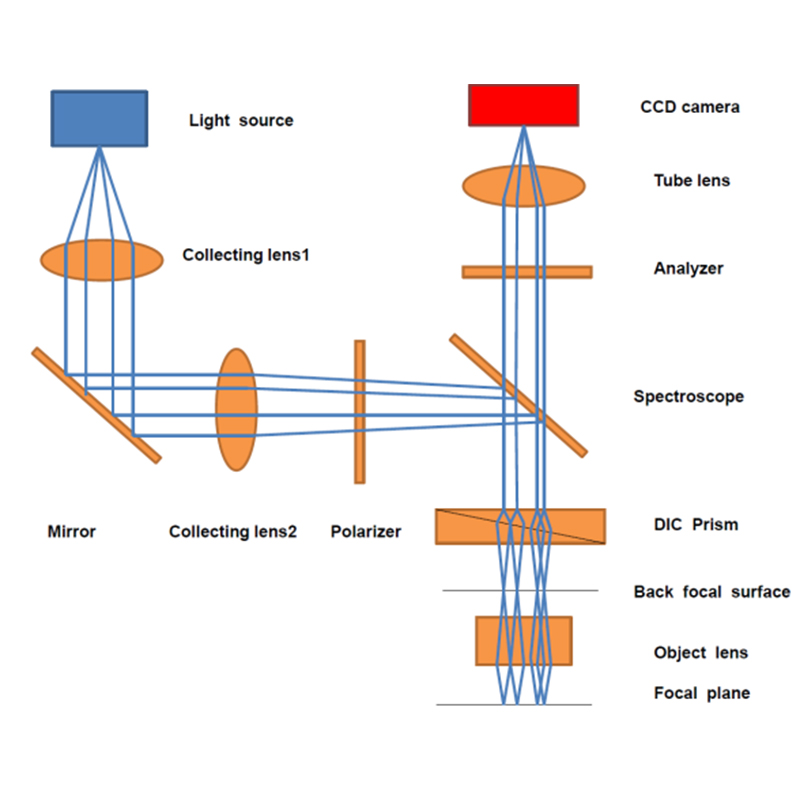
Differential Interference Contrast (DIC) microscopy works on the principle of coherent light interference, converting variations in sample surface topography into optical path differences. A position-sensitive detector measures intensity changes in the light wavefront, and digital signal processing derives the height variation of the sample surface. By adjusting the relative phase difference, the technique can also measure multiple optical path differences, yielding more detailed surface topography information. DIC microscopes are widely used in biological microscopy, semiconductor chip surface inspection, preparation and modification of nanomaterials, surface quality inspection of precision parts, PCB defect detection, and precision mold inspection, making them an important tool in modern scientific research.
2.Advantages of Differential Interference Contrast (DIC) Microscopy
Their advantages include high resolution, high precision, non-contact, and non-destructive measurement. Compared with conventional microscopes, DIC microscopes can achieve sub-nanometer resolution, enabling observation of finer surface structures and topographic changes. In addition, since the technique requires no contact with the sample, it eliminates sample damage and contamination, making it highly suitable for observing and studying biological and medical samples.
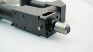
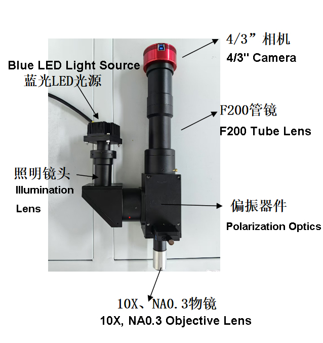
The DIC microscope developed by Wavelength Opto-Electronic features a compact, stable, high-rigidity body that meets the vibration isolation requirements of microscopic operations. Its modular functional design facilitates system upgrades. The guide-pillar lifting mechanism enables rapid adjustment of the distance between the stage and the objective, making it suitable for inspecting workpieces of varying thicknesses. Equipped with a mechanical moving stage, it effectively positions workpieces and is suitable for microscopic observation or rapid inspection of multiple samples. Its ergonomic design provides more convenient and comfortable operation with greater workspace.
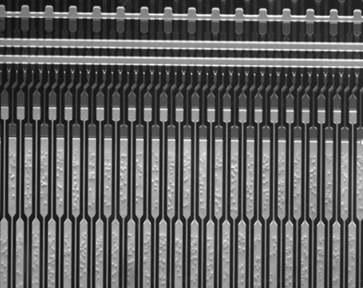
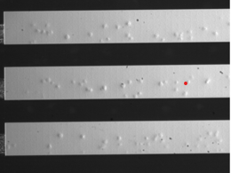
Conductive Particle Inspection on PCBs
3.Product Specifications
| Magnification | 10X |
| Working Distance (WD) | 32 mm |
| Resolution | 1.2 um |
| Parfocal Distance | 95 mm |
| Max Field of View | 4 mm |
| Thread | M26X0.706 |
| Numerical Aperture (NA) | 0.28 |
| Focal Length | 20 mm |
| Depth of Field (D.F) | 4.3 um |
| Entrance Pupil Diameter | 11.7 mm |
| Working Wavelength | 380-700 nm |
| Weight | 244 g |
| Magnification | 7X |
| Working Distance (WD) | 37 mm |
| Resolution | 1.6 um |
| Parfocal Distance | 95 mm |
| Line Pairs | 625 lp/mm |
| Objective Threading | M26X0.706 |
| Numerical Aperture (NA) | 0.22 |
| Focal Length | 28.6 mm |
| Cover Glass Thickness | None |
| Transmittance | 87% |
| Working Wavelength | 400-700 nm |
4.Applications of DIC Microscopy
1.Differential interference contrast (DIC) microscopy is widely used in biological imaging because it enables non-invasive observation of living cells without staining. It supports real-time visualization of cell interactions and protein dynamics when combined with fluorescence microscopy, and its pseudo-3D relief effect improves structural interpretation of tissues, organoids, and microorganisms.
2.In the semiconductor industry, DIC microscopy is used for precision inspection and process control. It helps detect microscale particles, residues, and etching defects on circuit boards and wafers, supports non-contact surface uniformity measurement, and enables process monitoring that reduces defect rates and improves manufacturing yield.
3.In materials science and nanotechnology, DIC microscopy supports nanoscale surface characterization, microstructure analysis, and nanofabrication process monitoring. It helps analyze height, roughness, and phase separation in metals, polymers, ceramics, and composite materials.
4.In precision engineering and manufacturing, DIC microscopy aids quality control of micromachined and electronic components. It is used for surface quality inspection, dimensional analysis of MEMS and optical parts, and high-resolution PCB defect inspection for solder joints, vias, and cracks.
Post time: Oct-06-2026